|
Thin-film
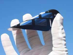
The three principal thin-film technologies are Amorphous Silicon (a-Si), Cadmium Telluride (CdTe) and Copper Indium Gallium diSelenide (CIGS). Amorphous Silicon (a-Si) Amorphous solids, like common glass, are materials in which the atoms are not arranged in any particular order. They do not form crystalline structures at all, and they contain large numbers of structural and bonding defects. Amorphous silicon applies to PV technology if the deposition conditions are properly controlled and if composition is carefully modified. Amorphous silicon absorbs solar radiation 40 times more efficiently
than single-crystal silicon, so a film only at 1 micron (one one-hundredth
of a centimeter) thick can absorb 90 percent of the usable solar energy.
Today, amorphous silicon is the most common form of thin-film PV and
is ideal for low-powered consumer devices. Cadmium Telluride, another thin-film technology, has cell efficiencies of over 16% in the laboratory. CdTe exhibits certain limitations that keep CdTe from full market acceptance, including Cadmium’s heavy metal characteristics and tendency to degrade electronic contacts outdoors. Also, CdTe deposition and crystal formation requires high processing temperatures. CdTe is only manufactured in a superstrate configuration in which sunlight must pass through the substrate to get to the PV material. Glass is the only material that can withstand the temperature and still be adequately transparent. Due to its fragile nature, the glass must be thick and heavy to endure the stresses found during product life in the field. Copper Indium Gallium diSelenide (CIGS) Copper Indium diSelenide (CuInSe2) has an extremely high absorption that allows 99 percent of available light to be absorbed in the first micron of the material. This makes it an optimal, effective PV material. Adding small amounts of Gallium to the CuInSe2 boosts its light-absorbing band gap, which makes it more closely match the solar spectrum, thereby improving the voltage and the efficiency of the PV cell. Consistently creating more electricity from the same amount of sunlight as other thin-film PVs, CIGS cells have reached conversion efficiencies of more than 19 percent - much higher than other thin-film PV. This high conversion efficiency remains stable over time for reliable performance. CIGS also passes environmental certification and waste-handling requirements.
 |
     |
 Rather
than growing, slicing, and treating a crystalline ingot as in crystalline
silicon manufacturing, thin-film technology uses the semi-conductor
characteristics of PV components to create PV material. Thin-film products
are made by sequentially depositing thin layers of the different materials
into a very thin structure, a process that requires very little semiconductor
material. Deposition is easier and less expensive than crystalline silicon
ingot-growth techniques.
Rather
than growing, slicing, and treating a crystalline ingot as in crystalline
silicon manufacturing, thin-film technology uses the semi-conductor
characteristics of PV components to create PV material. Thin-film products
are made by sequentially depositing thin layers of the different materials
into a very thin structure, a process that requires very little semiconductor
material. Deposition is easier and less expensive than crystalline silicon
ingot-growth techniques.
|
Copyright © 1998 - 2010 All Rights Reserved
|